A Premier B2B Part Search
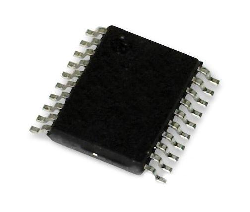
RENESAS 5V41067APGG Differential Clock Multiplexer
The IDT5V41067A is a high-performance 2:4 differential clock multiplexer designed for PCI Express Gen2 and Gen3 systems. It allows selection between two HCSL inputs with low additive jitter, supporting output termination to LVDS for compatibility with various devices. The device features a small 20-pin TSSOP package, operates at frequencies up to 200MHz, and includes an OE control pin for system power management. Optimized for demanding embedded applications, it ensures low phase jitter (<0.2 ps) and cycle-to-cycle jitter (<5 ps), making it ideal for reliable clock distribution in advanced high-speed interfaces.
RENESAS 5V41067APGG Differential Clock Multiplexer Specifications:
- Package: 20-pin TSSOP (173 mils)
- Operating Frequency: up to 200 MHz
- Additive cycle-to-cycle jitter: <5 ps
- Additive phase jitter (PCIe Gen2/3): <0.2 ps
- Outputs: 4 differential HCSL, 0.7V mode, can be terminated to LVDS
- Input Voltage: VDDIN 3.3V ± 5%
- Input Type: Differential TRUE and Complementary inputs
- Output Structure: Differential clock outputs driven in current mode
- Control Pins: OE (output enable), ASEL (input selection), PD# (power down), GND, VDD
- Temperature Range: -40°C to +85°C (industrial grade)
- Jitter: Cycle-to-cycle <5 ps, phase jitter <0.2 ps, suitable for high-speed clock distribution
- Power Management: OE pin for enabling/disabling outputs, power down feature included
- Material: Semiconductor compliant with industrial standards
- Certifications: RoHS compliant
Buy the IDT 5V41067A – Reliable PCIe Clock Multiplexer for Industrial Applications
Secure your system’s clock distribution with the IDT 5V41067A high-performance 2:4 differential clock multiplexer. Designed for PCI Express Gen2 and Gen3, it offers low additive jitter (<0.2 ps), cycle-to-cycle jitter (<5 ps), and a compact 20-pin TSSOP form factor. Its differential outputs are compatible with LVDS termination, ensuring versatile integration with high-speed devices. Featuring an active OE control pin for system power management, this device guarantees reliable, low-noise clock switching essential for demanding embedded and industrial applications. Purchase online today for precise and durable performance.
Get IDT 5V41067A today—built for precise high-speed clock multiplexing in demanding system environments.
Frequently Asked Questions
Where can I buy RENESAS 5V41067APGG?
You can click on the BUY or RFQ button to purchase 5V41067APGG from an authorized RENESAS distributor.
How do I troubleshoot issues or seek technical support for part 5V41067APGG?
You can download the 5V41067APGG datasheet or visit the RENESAS website for support.
Who is the manufacturer of 5V41067APGG?
RENESAS