A Premier B2B Part Search
RENESAS 5V41068APGGI8 PCIe Clock Mulitplexer
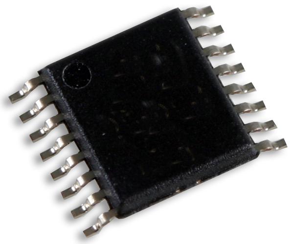
The IDT5V41068A is a 2:1 differential clock multiplexer designed for PCI Express systems, including Gen1, Gen2, and Gen3 applications. It features very low additive jitter suitable for high-speed systems, selecting between two differential HCSL inputs to drive a single differential HCSL output pair, which can also be terminated to LVDS. Its small 16-pin TSSOP package ensures a compact footprint, while the industrial temperature range supports demanding embedded environments. Key features include low cycle-to-cycle jitter under 5 ps and phase jitter below 0.2 ps at 200 MHz, making it ideal for high-performance clock distribution and system synchronization.
RENESAS 5V41068APGGI8 PCIe Clock Mulitplexer Specifications:
- Package: 16-pin TSSOP with dimensions approximately 7mm x 4.9mm
- Operating temperature: -40°C to +85°C (Industrial grade)
- Supply voltage: 3.3V ±5%
- Input voltage: ±0.7V differential, single-ended Vih ≥ 2.2V, Vol ≤ 0.9V
- Input capacitance: 15-27 pF, clock input differential impedance: 50Ω
- Output: differential HCSL, 0.7V, can be terminated to LVDS
- Additive cycle-to-cycle jitter: <5 ps, phase jitter at 200 MHz: <0.2 ps
- Output frequency: Up to 200 MHz
- Power consumption: Typical 40 mA at 100 MHz, with power-down current ~5 mA
- External components: 0.01 μF decoupling capacitors close to VDD pins, 50Ω resistors at outputs
- Outputs controlled via OE pin for power management, with internal pull-up
- Designed for PCIe systems, supports differential clock routing, and optimized PCB layout recommended
Buy the Buy IDT PCIe Clock Multiplexer Part Number 5V41068APGGI8 Online
Enhance your high-speed PCIe applications with the IDT PCIe Clock Multiplexer. Supporting Gen1, Gen2, and Gen3, this low jitter device ensures precise clock distribution. Its compact 16-pin TSSOP package fits easily on your PCB, while its industrial temperature range maintains reliable performance in demanding environments. Designed with low cycle-to-cycle jitter and phase jitter under 0.2 ps at 200 MHz, it reduces timing errors and enhances overall system stability. Order online now to get fast delivery and upgrade your system performance.
Order your IDT PCIe Clock Multiplexer Part Number 5V41068APGGI8 today and ensure high-speed synchronization for your PCI Express systems.
Frequently Asked Questions
Where can I buy RENESAS 5V41068APGGI8?
You can click on the BUY or RFQ button to purchase 5V41068APGGI8 from an authorized RENESAS distributor.
How do I troubleshoot issues or seek technical support for part 5V41068APGGI8?
You can download the 5V41068APGGI8 datasheet or visit the RENESAS website for support.
Who is the manufacturer of 5V41068APGGI8?
RENESAS